The ramping of chip manufacture on 300mm wafers and the move to ever small device design rules (130 nm and below) means the requirements on semiconductor manufacturing equipment are more stringent than ever. This means that each system component needs to be chosen carefully. AlN has excellently balanced properties for semiconductors equipment applications. These properties include excellent thermal conductivity, heat radiation and resistivity thermal shock tolerance and good insulating characteristics making this material an ideal match for cutting edge semiconductor capital equipment.
Features
| Features | AIN Materials | AlN | ||
|---|---|---|---|---|
| FAN-170 | FAN-200 | FAN-090 | ||
| 熱伝導率 | W/m·K(RT) | 170 | 200 | 90 |
| Heat radiation | (100ºC) | 0.93 | 0.93 | 0.93 |
| Thermal Expansion Coefficient | 10-6/ºC(RT~400ºC) | 4.5 | 4.5 | 4.5 |
| Volume Resistively | Ω·cm(RT) | >1013 | >1013 | >1013 |
| Dielectric Strength | kV/mm(RT) | 15 | 15 | 15 |
| Dielectric Constant | (1MHz) | 8.8 | 8.8 | 8.8 |
| Dielectric Loss | 10-4(1MHz) | 5 | 5 | 5 |
| Bending Strength | kgf/mm2 | 35 | 35 | 35 |
| Density | g/cm3 | 3.32 | 3.32 | 3.23 |
| Y | % | 3.5 | 3.3 | 0 |
| O | % | 1.5 | 1.2 | 0.58 |
| Total Metal Impurities | ppm | <500 | <500 | <500 |
| Features | Standard | High Thermal Conductivity | High Purity (Sintering Aidless) | |
Features
- High Thermal Conductivity and Heat Radiation, Excellent Thermal Uniformity
- High Thermal Shock Resistance
- Best Mach for Si wafer with Low Thermal Expansion.
- High resistance to fluorine corrosion
- High resistivity to for Plasma
Applications
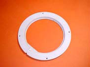
- Semiconductor Equipment (CVD,Etching) Susceptor, electrostatic chucks, Vacuum Chuck, Heater
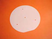
- Dummy Wafer
- Sputtering Targets
Specifications
| Size | (Max)φ/□550mm) |
|---|---|
| Thickness | 0.25to30(mm) |
*外形・Gradeによって別途相談になります。
Feel free to contact us!
Contact us from the form below. Our staff will reply soon!
Here to ask about AIN Ceramics for Semiconductor Equipment